Altium pcb designer: 2013 Altium designer tutorial: step by step guide Altium layers documentation signal layer
Gaining Insight into Your PCB with Color Displays | Altium
Altium color designer Altium 3d mode change inside background default configuration workspace start end Altium ckt schematics
Altium designer tips and shortcuts
Altium designer tips #19: how to set net color in altiumHow are these layers like lcd added in altium designer? Layers routing altium controlled configurationsThe routing.
Altium pcb routing managing howie vaultAltium 3d designer pcb model Altium designer tutorial step guide documentation installing sourceLcd altium.

Altium sheet size designer set
Whats new in altium designer 6.0Altium designer Traces altium brighter netsAltium tutorial-1:how to design schematics in altium /complete details.
Altium shortcutsHow to change the default white background in 3d mode inside altium How to set the sheet size in altium designer?Pcb color altium displays visual insight gaining into barrier breaking overrides colors help.

Gaining insight into your pcb with color displays
[altium] why are some traces are brighter than other traces? why isn'tManaging design changes between the schematic & the pcb in altium Pcb lvds differential pairs altium pair schematic twisted crossed wires designer meaning fpga correctly allowable device map pins level usedAltium designer.
View configurationHow are these layers like lcd added in altium designer? .


How to change the default white background in 3D mode inside Altium

How are these layers like LCD added in Altium Designer? - Electrical
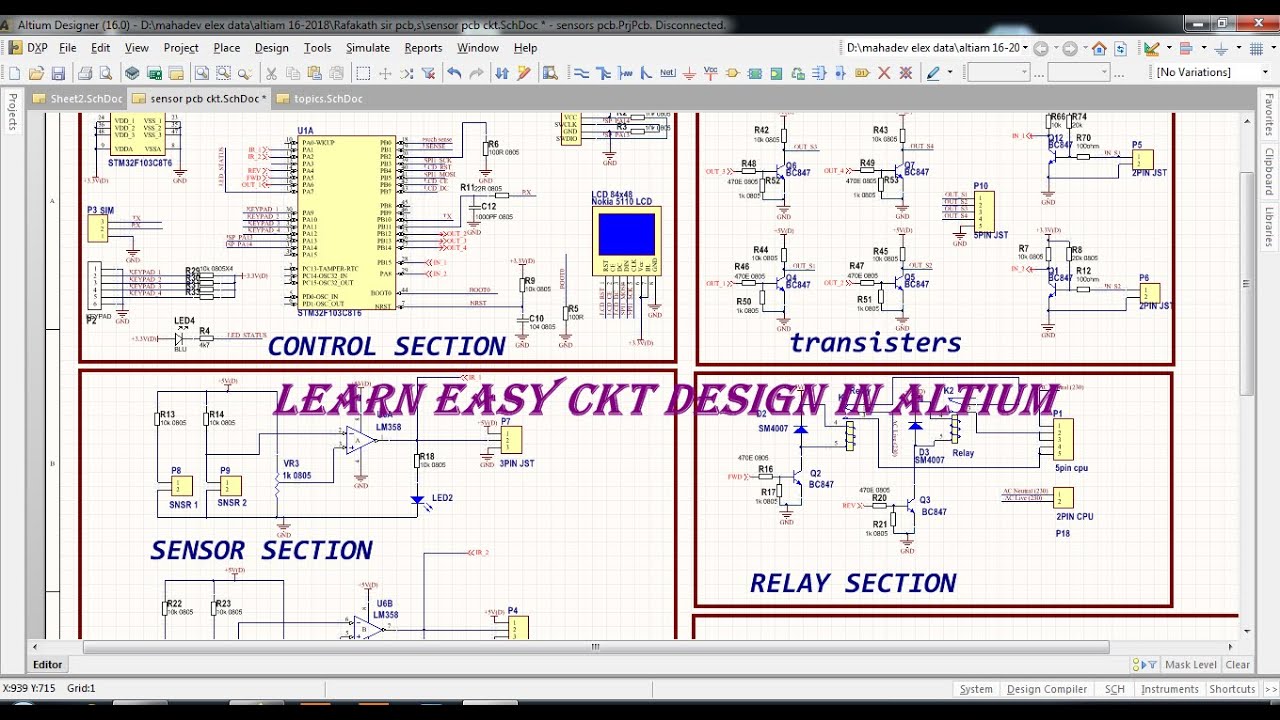
ALTIUM TUTORIAL-1:How To Design Schematics in ALTIUM /Complete details
![[Altium] Why are some traces are brighter than other traces? Why isn't](https://i2.wp.com/external-preview.redd.it/FhUvZtBXqld44uuzGUisVnilCLQ1GdH5v6go1xk0XQc.png?width=960&crop=smart&auto=webp&s=dd521bde5f2fe4281cc8aec6df66c5cb9585ecc5)
[Altium] Why are some traces are brighter than other traces? Why isn't

Altium Designer - 3D model of your PCB - it's really easy - YouTube

How to set the sheet size in Altium Designer? - Electrical Engineering

Altium PCB Designer: 2013

View Configuration | Online Documentation for Altium Products

Whats New in Altium Designer 6.0 | Online Documentation for Altium Products